If you’ve ever worked with PCBs for any length of time—whether you’re an engineer designing the next big consumer gadget, a product manager trying to get a medical device to market on schedule, or a manufacturing lead juggling a dozen parts at once—you know how gut-wrenching it is when a production line grinds to a halt because a random batch of boards keeps failing out of testing. Last year, we had a client call us panicking because 12% of their prototype PCBs were failing thermal cycling tests, and they had a launch date 6 weeks away. They’d already swapped solder suppliers, changed reflow profiles, and even bought new components, but nothing stuck. That’s where PCB assembly failure analysis comes in—and for guys like us, who live and breathe getting boards right, it’s way more than just diagnosing a broken part. It’s the safety net that keeps production on track, costs from spiraling, and customers from tearing their hair out. PCB Assembly
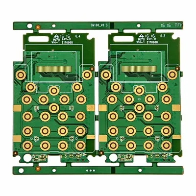
Let’s cut through the jargon first: failure analysis (FA) in PCB assembly isn’t just “looking at a broken board under a microscope.” It’s a structured, step-by-step process we walk through every time a batch of boards doesn’t meet specs, a finished product crashes mid-use, or a prototype test fails. Our job as an assembly supplier isn’t just to solder parts down and ship them. We’re with our customers from the first prototype run all the way to full production, and FA is the thing that turns “we had no clue why this failed” into “here’s exactly what went wrong, and how to fix it so it never happens again.”
Let’s break down what that actually looks like in real life, not some textbook example. First, we start with what we call “non-destructive testing” (NDT) because the last thing we want to do is ruin a good sample and make a customer wait longer for a fix. That means we pull out tools like X-ray to see what’s going on inside joints you can’t see, optical microscopes to look for tiny solder bridges or misaligned parts that are too small for the naked eye, and thermal cameras to check if a component is overheating when it’s powered on. On that same prototype run I mentioned earlier, when we put the faulty boards under X-ray, we noticed the solder joints on the BGA (ball grid array) chip—those tiny, hard-to-see connections under the chip—were forming voids that were way bigger than the industry standard. The voids weren’t just empty space; they were disrupting the thermal path between the chip and the board, so when the device cycled from hot to cold, the joints expanded and contracted unevenly until they cracked. The customer had no way to see that because you can’t pop a BGA up to check its joints without special tools. That’s the first big role of FA: it reveals problems you can’t spot with visual checks alone.
Next, we move to more targeted testing, and here’s where FA earns its keep for our production customers, not just prototypes. Say we’re building 10,000 PCBs for a home appliance, and 0.5% of them fail a connectivity test. We can’t just scrap all 10k boards— that’s hundreds of thousands of dollars down the drain. FA lets us narrow down the root cause fast, before we waste more money. In that appliance example, we might do a cross-section of a faulty solder joint to see if there’s a problem with the solder paste stencil (the metal mask we use to apply solder) that’s putting too much or too little paste in certain areas, or if the reflow oven temperature was inconsistent across the board (common if you cram too many boards on a tray for baking). Last quarter, a client had a batch of smart thermostat PCBs that were failing after 500 hours of field testing. We pulled 20 faulty boards and 20 working ones, compared their material composition, and found the dielectric layer on the PCB substrate was thinner than the customer had specified, so it couldn’t handle the voltage from the power supply. We worked with the substrate supplier to adjust their manufacturing process, and that fixed the issue before the client lost shelf space at big box stores. Without FA, they would have kept blaming their component supplier or their firmware, which would have led to months of delays and way higher costs.
Another big, underrated part of FA is separating assembly mistakes from design or component issues. This is the part that keeps our relationship with customers honest, because we don’t want to take the blame for something that’s not our fault, and we don’t want a customer to blame us when their design has a flaw. For example, a client once brought us a batch of PCBs where resistors were falling off the board during wave soldering. At first, we thought we’d messed up the solder profile—so we tested 50 boards, reflowed them three different ways, and still had 10% fall off. Then we looked at the resistor footprint on the customer’s design: it was too small, so there wasn’t enough solder to hold the resistor when the board moved through the wave. FA let us prove that the problem wasn’t our soldering process—it was the footprint design—and we gave the customer a free modified footprint for their next run. That saved them hundreds of dollars in rework and kept us from getting a bad rep for a mistake that wasn’t ours. We’ve had the opposite happen too: a client thought their ceramic capacitors were failing because of design flaws, but FA traced it back to a bad batch of capacitors that had internal cracks from being dropped during shipping. We helped them set up proper shipping protocols, and the problem went away. FA turns guesswork into facts for both sides, which is huge for trust.
For prototype and R&D customers, FA is even more critical. When a startup is trying to get their first product to market, they don’t have a team of fault analysts on staff— they’re just a handful of engineers working late nights in a garage. We’ve had clients bring us a prototype with a weird intermittent fault: it works for an hour, then dies, and they can’t replicate it in the lab. That’s the hardest type of failure to diagnose, because it only shows up under real-world conditions. We use things like accelerated life testing—putting the board through cycles of temperature, vibration, and humidity that mimic 5 years of use in a car or a phone—to trigger the fault faster, then use data loggers to track every variable while it runs. On one drone prototype, we found that the power supply pin on the microcontroller wasn’t coated properly, so when the drone was flown in high humidity, moisture seeped into the pin and caused a short. Fixing the coating took 2 days, and the client was able to test their drone for a trade show that was 3 weeks away. Without FA, they would have had to scrap the prototype and delay the entire launch.
Let’s talk about the cost part, because that’s what gets decision makers’ attention. The average cost of a PCB assembly failure that’s caught after full production is anywhere from $10,000 to $100,000, depending on the product. A medical device failure, for example, is way more expensive because of regulatory requirements—you can’t just fix the boards; you have to file paperwork with the FDA, recall units, and prove the fix works, which costs millions. FA cuts that cost drastically because it lets us fix the root cause before it becomes a full-blown issue. On that thermostat batch I mentioned earlier, FA let us fix the substrate issue in one run, so the client only lost a few hundred dollars in testing fees instead of millions in recalled units. For startups, FA is often the difference between staying in business and folding—delays of even a month can mean missing a funding round or a holiday sales window that makes or breaks a product.
Here’s the thing about FA that a lot of people don’t get: it’s not just about fixing the current problem. It’s about preventing future ones. After we diagnose a batch failure, we update our process checks to catch similar issues early on. For example, when we found that BGA voids were causing the thermal cycling failures, we added an extra X-ray check for all BGA boards before they leave our facility, so we don’t ship out boards that have dangerous voids. We also share the findings with our other customers who use BGAs, so they can add the same check to their production runs, which helps them avoid the same problem. That’s the collaborative part of FA—we’re not just a supplier that sells boards; we’re a partner that helps our customers make better products.
Now, I know some people will read this and think “why not just test every board?” Testing every board takes time, money, and it’s not even possible for small, intermittent faults that only show up after hours of use. FA is targeted—we only test what we need to, so we get answers fast without wasting resources. And for every batch that fails, we might have a dozen that pass without any issues, so FA is focused on the outliers that can derail everything.
At the end of the day, the role of PCB assembly failure analysis for us as a supplier is simple: we turn chaos into clarity, uncertainty into solutions, and delays into progress. We’ve all been in that spot where a project is falling apart because no one can figure out what’s wrong, and FA is the tool that pulls us out of that hole. It’s not glamorous—most of the time we’re hunched over microscopes or staring at X-ray images at 8 PM—but it’s the most important part of our job, because it’s what makes our customers trust us to get their products to market right, on time, and without breaking the bank.
If you’re working on a PCB project, whether it’s a prototype, a pilot run, or full production, and you’ve hit a snag that no one can figure out, we can help. We’ve worked with startups, industrial companies, medical device makers, and consumer electronics brands to diagnose everything from tiny solder voids to design flaws to bad component batches. Let’s talk through your issue—no jargon, no pushy sales pitches, just straight answers to get your project back on track.
Prototype PCB Assembly References
- Electronic Industries Alliance. (2018). PCB Failure Analysis: Principles and Practices. EIA Standard IPC-TR-579.
- Lall, P., et al. (2020). Root Cause Analysis of Solder Joint Failures in High-Density Interconnect PCBs. IEEE Transactions on Components, Packaging, and Manufacturing Technology.
- Williams, K. R. (2021). The Cost of PCB Assembly Failures: A Guide for Manufacturers and Design Engineers. Journal of Electronic Manufacturing.
Huaswin Electronics Technology Co., Ltd.
Address: Building A2, Hao Hai Hong Industrial Park, No.3 Yu He Road, Gong He, Sha Jing, Bao An, Shenzhen
E-mail: sales@huaswin.com
WebSite: https://www.huaswin-pcba.com/
